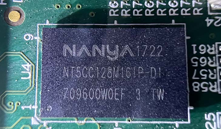
NT5CC128M16IP-DI is a DDR3 memory chip on the S9 control board, which can realize high-speed operation. It is internally configured as eight banks of DRAM. 2Gb chips are organized as 32Mbit x 8 I/O x 8 bank or 16Mbit x 16 I/O x 8 bank devices. These synchronous devices enable high-speed double data transfer rates up to 1866Mb/sec/pin for general-purpose applications.
The chip is designed to meet all key DDR3(L)DRAM key features, and all control and address inputs are synchronized to a pair of externally supplied differential clocks. The inputs are latched at the crossing points of the differential clocks (CK rising and CK falling). All I/Os are source synchronous with single-ended DQS or differential DQS pairs.
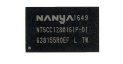
Product feature:
• Compliant with JEDEC DDR3
- 8n prefetch architecture
- Differential clock and data strobe
- Double Data Rate on DQ, DQS and DM
• Data integrity
- Automatic Self-Refresh (ASR)TS with built-in DRAM
- Auto Refresh and Self Refresh Mode
• Power saving mode
- Partial Array Self Refresh (PASR)
- power down mode
• Signal integrity
- Configurable DS for system compatibility
- Configurable on-chip termination
- ZQ calibration for DS/ODT impedance accuracy via external ZQ pads (240 ohms ±1%)
• Signal synchronization
- write leveling via MR settings
- read leveling via MPR
• Interface and power supply
- SSTL_15 for DDR3: VDD/VDDQ=1.5V(±0.075V)
- SSTL_1353for DDR3L: VDD/VDDQ=1.35V(-0.067/+0.1V)


 71464.14USD
 53.96USD
 1.34USD
 0.09USD
 2192.32USD
 8.39USD
 601.43USD
 82.51USD
 0.05USD
 0.03USD
 0.04USD
 Favorites
 History

 Feedback
