63202.64USD
 43.94USD
 1747.11USD
 0.03USD
 7.03USD
 570.03USD
 0.02USD
 78.11USD
 0.04USD
 1.1USD
 0.07USD
 Favorites
 History
 Feedback
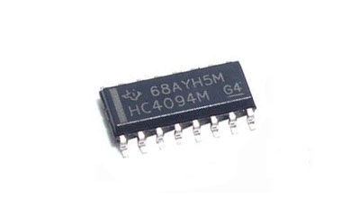
CD74HC4094M96
CD74HC4094M96 parallel output can be directly connected to the public bus. The data is shifted during the positive clock transition. When the Strobe input is high, the data in each shift register stage is transferred to the storage register. Whenever the OE signal is high, the data in the storage register will appear at the output. Two serial outputs can be used to cascade multiple of these devices. Data is provided on the QS1 serial output terminal on the rising edge of the clock to allow high-speed operation in a cascaded system where the clock rise time is very fast.
Logical series/base: 74HC4094
Shift register function: serial to parallel, serial to serial
Number of elements: 1 element
Number of bits per element: 8 bits
Logical case style: integrated circuit
Number of pins: 16 pins
Minimum power supply voltage: 2V
Maximum power supply voltage: 6V
IC output type: Three states
Logic IC series: 74HC
Logic IC base: 744094
Minimum working temperature: -55°C
Maximum working temperature: 125°C